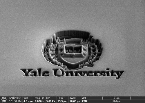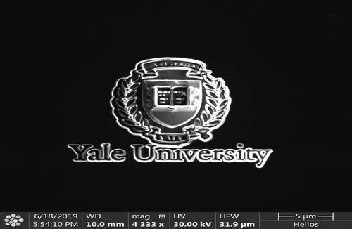

For the first time the Yale insignia receives the “FIB SEM” treatment at the Materials Characterization Core. In just a few moments, the surface of a silicon chip, around the thickness of a human hair, is milled with unprecedented precision, please check the video here. The new technology is enabling scholars to examine materials at least 100x smaller.
The arrival of the Focused Ion Beam Scanning Electron Microscope or “FIB SEM” at Yale’s West Campus is empowering scientists to investigate materials not just with surgical precision, but with atomic precision. Being able to view surfaces only a few atoms thick, identify key topological features, probe elemental composition, and quickly mill (or sputter) nanoscopic layers, the sophisticated technology is making it possible for scientists at the Energy Sciences Institute and across Yale to characterize the functionality of new materials and to produce minute components for future energy production and storage.
The milling was performed by Lei Wang during final testing of the system. Visit https://ywcmatsci.yale.edu/ to find out more.